Device Fabrication
Organic Material and Metal Growth
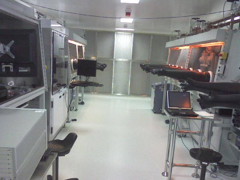
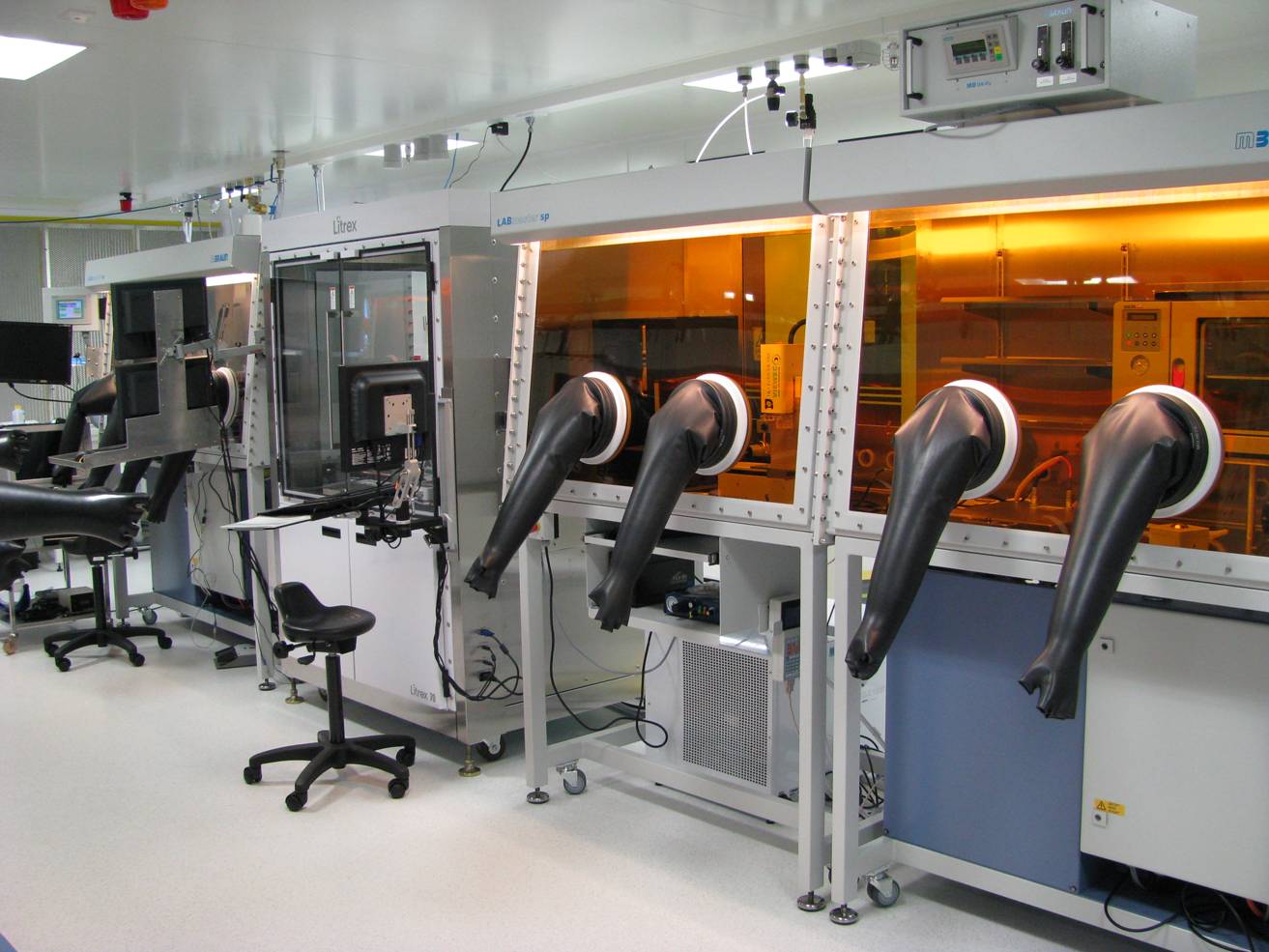
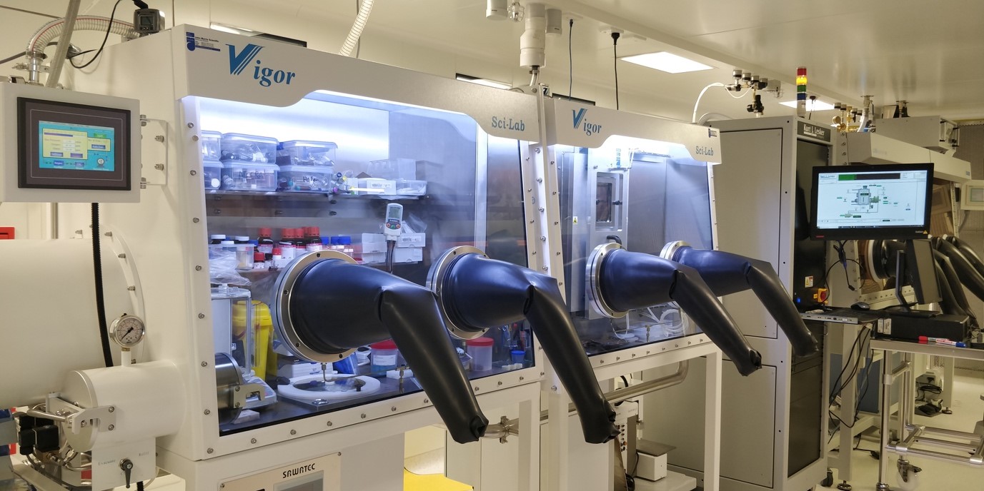
The Centre has four separate deposition systems with one for general device fabrication with the remaining two dedicated to photovoltaic/photodiode or OLED fabrication. Each of the systems has the capability for solution coating organic semiconductor inks in integrated gloveboxes. All the glove boxes have a nitrogen environment with O2 and H2O content of less than 1 ppm.
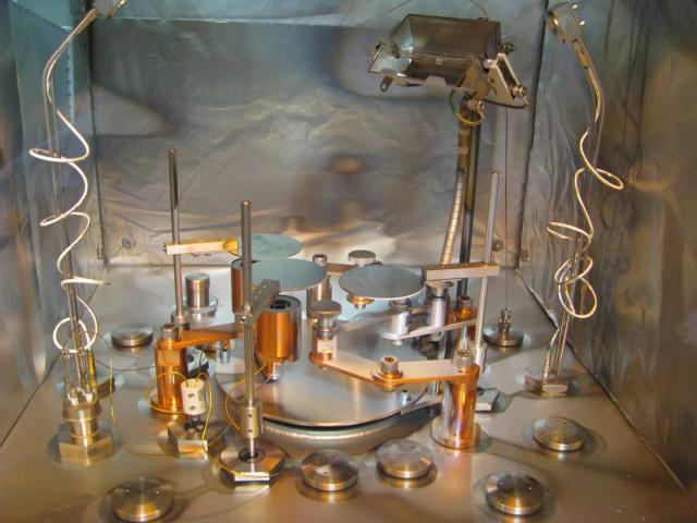
The first evaporation system is equipped with two high-vacuum evaporation chambers.
The first one has two organic evaporators (up to 600 °C) and two thermal evaporators for metal and dielectric. The second one has three thermal evaporators and DC sputter head.
The OLED evaporation system has 6 low-temperature organic sources supporting co-evaporation with rate control and 4 high-temperature metallic/inorganic sources. The evaporator can take substrates with a maximum size of 150mm x 150 mm substrate and deposit with uniformity within 5%.
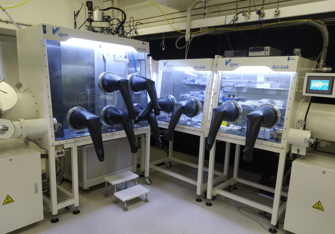
The photovoltaic/photodiode evaporator system has OPV and perovskite device fabrication system has 4 low temperature evaporation sources for organic materials and 2 high temperature evaporation sources for metals/inorganics with a maximum substrate size of 100 mm x 100 mm.
Characterisation Facilities
The Centre has many different device characterisation systems such as:
- Two solar simulators and I-V and IPCE systems, one is installed inside the cleanroom and measurements are carried out inside a glovebox. This is part of the ANFF-Q equipment and is used for testing air-sensitive solar cells. The second one is installed inside the optical lab for testing organic and inorganic solar cells.
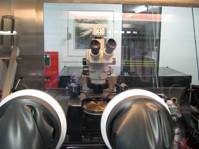
- A semiautomatic probe station and Agilent B1500A characterisation system are used for testing electrical properties of electronic devices such as thin film transistors. The probe station is located inside the glovebox.
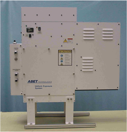
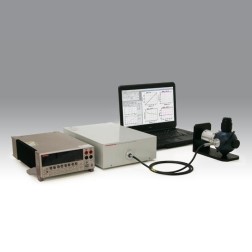
OLED External Quantum Efficiency measurement system (Hamamatsu C9920-12) that is comprised of an integrating sphere with 3.3” inside diameter and PMA-12 Photonic multichannel analyser (200 nm to 950 nm BT-CCD detector) enabling all key OLED characteristics to be collected simultaneously.
